Credit Source

Imec has unveiled a new climate-friendly way to produce patterns on chips using lithography and etch for advanced chip factories.
Leuven, Belgium-based Imec said the tech can reduce the carbon dioxide footprint of lithography and etch for advanced technology nodes for chip factories.
Photolithography is a key part of the process of manufacturing of integrated circuits, or semiconductor chips. It uses light to transfer a pattern onto a substrate, typically a silicon wafer, almost like printing a design on top of a chip surface.
Imec said it could significantly reduce the carbon footprint associated with lithography and etch processes in semiconductor fabrication. The announcement was made during the 2024 Advanced Lithography + Patterning Conference, where Imec presented sustainable alternatives and practices to curtail direct emissions of CO2 in these critical processes.
GB Event
GamesBeat Summit Call for Speakers
We’re thrilled to open our call for speakers to our flagship event, GamesBeat Summit 2024 hosted in Los Angeles, where we will explore the theme of “Resilience and Adaption”.
Apply to speak here
Imec’s research indicates that lithography and etch processes contribute over 40% of direct emissions in advanced logic node Scope 1 and Scope 2 categories. Semiconductor devices produced in 2021 generated a CO2 equivalent footprint of about 175 megatonnes, equivalent to the yearly emissions associated with about 30 million people.
Imec’s alternatives include ways to simplify the dry etch processes widely used in chip manufacturing. The aim is to reduce the environmental impact of these processes while maintaining high-quality semiconductor fabrication.
Imec.netzero Virtual Fab Model
Imec.netzero, a virtual fab model developed within Imec’s Sustainable Semiconductor Technologies and Systems (SSTS) program, played a pivotal role in demonstrating the emissions impact. Imec showcased the contributions of lithography and etch processes to Scope 1 and Scope 2 emissions, emphasizing the need for innovative solutions.
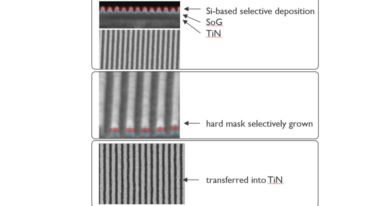
Imec proposes directions for future patterning, including ultra-thin resists and underlayers, minimal passivation, and low process temperatures for etch. A High-NA-compatible metal line etch process was demonstrated, showcasing a significant reduction of approximately 94% in process gas emissions.
Addressing lithography challenges
Challenges in lithography include emissions associated with electricity generation. Engineers have tried using greener energy, reducing multi-patterning steps, minimizing photoresist dose, and enhancing scanner throughput for energy efficiency.
“Sustainability is important for Imec and we are pleased to see that it is also gaining importance at the SPIE Advanced Lithography and Patterning conference,” said Emily Gallagher, a principal member of the technical staff at Imec, in a statement. “An informal search of papers shows a promising trend: in 2018 there was only restricted one paper that mentioned sustainability and now, only six years later, the conference is anticipating 45 papers in the sustainability track, four of them coming from Imec. Last year
shattered global climate records, so it is essential that we all take action as organizations and as individuals. Imec has embraced this action at all levels including our research.”
Imec’s initiatives in process innovation and sustainability reflect a broader industry shift towards eco-friendly semiconductor fabrication.


/cdn.vox-cdn.com/uploads/chorus_asset/file/25307299/Stardew_Valley_1.6_update.jpg)
